Amplifier Topologies for Current-Drive
An amplifier that converts input voltage into output current is generally called a transconductor, and the symbol of transconductance, i.e. the ratio of output current to input voltage, is usually gm. However, the term "amplifier" is still quite appropriate since both current and power are at the output always greater than at the input.
The Series Resistor Method
The simplest means to establish a transconductor in practice is to connect a series resistor at the output of a coventional voltage amplifier. The higher the resistance with respect to the speaker impedance, the purer the amplifier operates in the current-drive mode. The obvious drawback is, of course, that available output power is drastically recuced, and thus the method suits mostly only for experimenting.
If you try this with a conventional voltage mode loudspeaker, you are likely to observe both good and bad changes in sound quality. The good ones are due to the fact that the electromotive forces (EMFs) generated by the speaker drivers are now less able to disturb the current flowing through them. The possible adverse effects are due to the unfavorably changed frequency response, usually in the bass region and near crossover points where the speaker impedance has peaks. (Of course, it is possible that some part of the favorable changes are also related to frequency response.) If you have access to a graphic equalizer or DSP, you can possibly compensate these response alterations and keep only the benefits.
Basic Current-Feedback
Virtually all audio power amplifiers in use today are implemented by the basic scheme shown in figure a below, that is, using voltage feedback. (If you look at any schematic of a power amplifier, you can distinguish the two resistors connected from the output node to the other input transistor and from there to signal ground.) The signal to be amplified, Ui, is applied to the non-inverting input of a differential amplifier (triangle), and a specified proportion of the output voltage Uo, as determined by resistors R1 and R2, is brought back to the inverting input. Ideally, the circuit always sets its output voltage so that the difference voltage, Ud, remains at zero. Voltage at the common point of the resistors is then Ui, and because no significant current goes to the input terminals, the voltage division causes Uo to follow Ui, amplified by the factor (R1+R2)/R1.
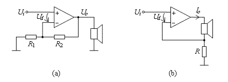
Figure b shows, correspondingly, the use of current-feedback* in its simplest form. Again, the non-inverting input terminal acts as the input, but now the feedback signal applied to the inverting terminal reflects the current flowing through the load (Io), instead of the load voltage.
The operation of the loop can be conceived as follows: Suppose the difference voltage Ud is, for some reason, growing positive. The differential amplifier responds to this by raising its output voltage, making thus current Io and the voltage drop in R change in the positive direction. This increase continues until the feedback signal reaches the input signal and Ud is nulled. Likewise, when Ud is becoming negative, Io and the voltage of R decrease until the deviation in Ud has been eliminated. Because the resistor's voltage thus follows the input voltage, we obtain as the circuit's transconductance gm = Io/Ui = 1/R.
A suitable value for R is about half an ohm. With such a value, the power consumed in the resistor generally amounts to less than a tenth of the power taken by the speaker, so the loss is not very significant.
Above, we assumed that the difference voltage Ud stays at zero which requires an ideal differential amplifier. A real differential amplifier has, however, only finite gain (designated Ad), that falls off with increasing frequency. Also, the output of any differential amplifier always has some internal impedance (designated Zo) even though it is generally not directly specified.
The transconductance with a real differential amplifier can be shown to be

where ZL is the load impedance. As Ad is high in absolute value, Zo and ZL become negligible, and we are left with gm ≈ 1/R, as in the ideal case. It is important that the transconductance's (and hence the current's) dependence on the load impedance ZL is made small, and this is achieved when |Ad| and R are high enough.
The output impedance (total impedance seen by the load) achieved by the circuit is

Thus, Zo being small, the output impedance is about directly proportional to the differential gain. If R is 0.5 Ω and |Ad| is at 20 kHz yet 500, as common, the minimum value of |Zt| will be a good 250 Ω, which is, in practice, very satisfactory.
*The term 'current feedback' is also used to denote a certain feedback arrangement where the inverting input terminal is of low-impedance type and thus sinks or sources current. Some manufacturers also use this scheme in audio amplifiers, but this has nothing to do with feeding the load by current.
Ensuring Stability
At high frequencies, the inductivity of the speaker and its cable causes (See fig. b above) the feedback signal to exhibit certain phase lag with respect to the output voltage. This phase lag adds to the total lag of the loop and can hence jeopardize the circuit's stability although there would be enough voltage gain for stable operation with resistive feedback. In order to make the feedback more resistive at high frequencies, an RC network can be attached in parallel with the speaker, as shown in the figure below; this arm acting like an extra "way" in a crossover filter and establishing the principal current path for the highest frequencies. It is better to connect the arm in the amplifier rather than in the speaker, so that cabling inductance will also be eliminated. (It is common practice also in conventional amplifiers to use an RC branch from the output to ground though its function is different.)
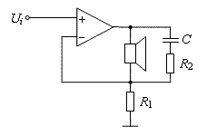
A strongly capacitive load may also make some amplifier circuits oscillate, and the presented RC arm also helps in such a case. Additionally, the arm constrains possible high-frequency noises, whose leading to the speaker is not meaningful.
Grounded Load Operation
If so desired, the load can be attached to the ground by using the variation shown below in which the load and the current-sensing resistor have been interchanged. Because this resistor is now separated from the ground, its voltage drop has to be replicated into a ground-referenced feedback signal with a distinct difference amplifier, consisting of A2 and four resistors.
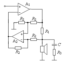
From the standpoint of the power amplifier (A1), nothing else has changed, except that at high frequencies the difference amplifier introduces in the feedback signal some extra phase lag, that may have effect on the circuit's stability. To prevent the danger of oscillation, A2 should thus have quite a large bandwidth (like e.g. NE5534).
Using One-Sided Supply Voltage
The topology below is suitable for one-sided supply voltage. At the operating frequencies, the circuit employs current-feedback but changes to voltage feedback below the operating band, so that the output would not be saturated by the direct voltage accumulating in C3.
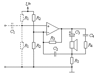
The voltage alterations of the current-sensing resistor R5 are shifted by C2 to the inverting input to form the current-feedback. C2 as well as C3 and C4 assume half of the supply voltage. C2 has to be so large as to exhibit negligible impedance, at the operating frequencies, compared to resistances R2 and R3.
An important additional benefit of the current-drive operation is that the non-idealities of the electrolytic capacitor (C3), that is needed for DC blocking, are not able to affect the load current and hence to degrade sound quality, as can happen in a voltage-output amplifier. Also, the current-driven capacitor does not introduce a pole (i.e. a roll-off) in the low-frequency response, as happens in conventional design.
Bridging
The concept of bridging, much employed in voltage amplifiers, is also applicable to current-drive systems. Below is shown a bridge-connected transconductor topology, in which one power amplifier (A1) controls the current flowing through the load while an other (A2) mirrors the output voltage of the former to opposite polarity. A3 and resistors labeled R2 make up a difference amplifier that provides a load current dependent feedback signal similarly as above in the grounded load case.
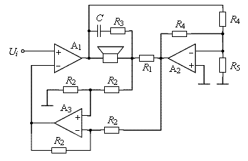
The current taken from the output of A1 can now be 2-fold compared to a corresponding unbridged circuit, and the value of the current-sensing resistor (R1) can be half of that one would use without bridging.
In terms of stability, the bridged circuit is somewhat more demanding than the usual. Of course, the difference amplifier and the inverting amplifier must in themselves be stable. In addition, A1 has to keep stable despite the phase lags developing in the aforementioned amplifiers at high frequencies. (Further instruction found in the book.)
The Modified Howland Circuit
Another usable way to realize transconductance amplifiers is the so-called improved Howland current pump, that is represented in the figure below. Here, we also have a kind of current-feedback, but now the difference voltage is established by means of resistor divisions.
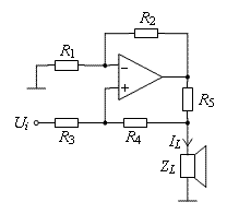
The load can be ground-connected without additional arrangements, but, as a small inconvenience, resistors need to be precisely matched to achieve the maximum output impedance. The circuit can also be made inverting by applying the signal via resistor R1 and connecting R3 respectively to ground.
Matching is achieved by satisfying the following condition:

R5 acts as the current-sensing resistor and has thus very low value compared to the other resistors. Hence, the equation is, in practice, satisfied fairly well even by choosing equal values for all resistances from R1 to R4. The resistors should be matched preferably to 0.1% to achieve good performance.
When the matching condition is met, the transconductance can be shown to be

Thus, when R1 and R2 are equal (implying R3 and R4 are also equal), the transconductance will be the reciprocal of the sensing resistor's resistance, as also in the basic topology.
The output impedance achieved by the topology can be shown to be

Thus, Zt is also here directly proportional to the differential amplifier's gain. However, due to the factor R1/(R1+R2), |Zt| always remains a little lower than in the first-discussed basic transconductor with the same sensing resistor value.
The stage preceding the Howland circuit must have very low output impedance because it directly adds to resistance R3. Therefore, the feed must be taken directly from an operational amplifier output.
In stability properties, the improved Howland circuit does not differ remarkably from the simple current-feedback. Thus, the RC compensation branch in parallel with the speaker (though not shown) is here as recommendable as elsewhere.
Voltage Regulators as Controlled Current Sources
Adjustable voltage regulators also make a convenient way to implement current amps. Positive adjustable regulators usually exhibit sufficiently low distortion and can be easily used to make controlled current sources. Negative ones, however, are much poorer in ripple rejection performance at high frequencies and therefore not so usable.
Below are shown the basic schemes for such sources. Figure 'a' shows a constant-current source capable of being used at both ends: node A can be connected to a supply potential while node B acts as a current source, or B can be at a supply potential while A acts as a current sink. Current flowing from the regulator's adjustment pin is constant at about 50 uA and can thus be ignored. Current I, which therefore must be equal at the IN and OUT pins of the regulator, always equals the regulator reference voltage (1.25V) divided by the current-setting resistance R.
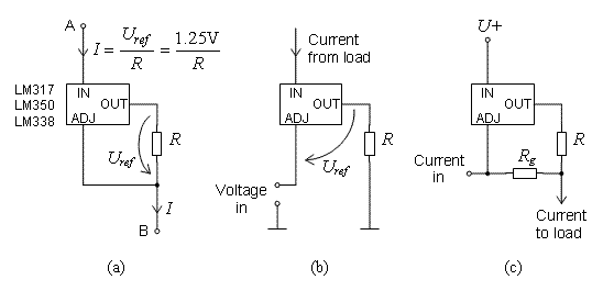
Figure b shows the usage as a voltage-controlled current sink. The input voltage becomes added as such in the voltage across R which determines the current through the regulator. To keep the DC levels moderate, the input voltage needs to travel below the supply rail, but this is not a problem.
In fig. c is pictured a floating current-controlled current source. The input current fed through the gain resistor Rg develops a voltage drop in it that alters the voltage across R, hence controlling the current that flows to the load.
By combining these blocks we can construct class A current source amplifiers without the usual means of placing a current feedback over a voltage-delivering amplifier. There is still negative feedback inherent in the regulators, but the load seen by the feedback systems remains always resistive. A remarkable benefit is also that in a bridged system the other side can be even a low-performance class B voltage amplifier because the current through the load is solely determined by the transconductor side.

