Transconductance Amplifier
With Adjustable Resonance and Baffle Step Compensation
In the following are given building instructions for a current-output stereo amplifier capable of delivering about 12 watts into 8 Ω load. The power stage is based on TDA2040, whose properties are suitable for the purpose and that worked in testing reliably at all signal levels. LM1875 is pin compatible and should also be a proper alternative but has not been verified. The power supply is regulated and common for all stages and both channels.
Harmonic distortion measures 0.18% at 10 W and 0.003% at 1 W with 8 Ω load.
If more power is needed, TDA2050 can be used instead, with some modifications to the circuitry.
Structure
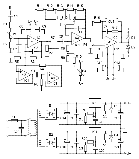
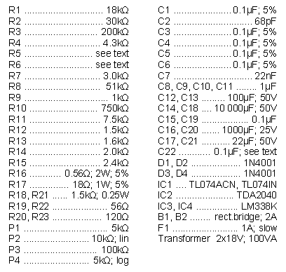
Below is shown the schematic of the amplifier with a suitable voltage supply, the corresponding parts list being given in the table. In addition to the transconductor stage, the amplifier incorporates a novel resistor-tunable resonance cancellation circuit based on the pole shifting technique (often referred to as the Linkwitz transform) and an adjustable active baffle step compensation for loudspeakers without this correction. Both functions can also be bypassed to provide flat frequency response.
Input Attenuator
The intaken signal is attenuated at the beginning somewhat by voltage divider R1-P1-R2, so that voltage at the outputs of A1 and A4 would not become clipped in any situation despite that the resonance compensation stage (A1 with its feedback network) amplifies the lowest frequencies strongly. Overdrive should not occur if the peak values of the input signal are 3 V at most and the resonant frequency of the driver to be equalized (fz) is 80 Hz at most. Trimmer P1 is used for fine-tuning the channel sensitivities to equal levels.
Bass Equalization
A1 with its feedback network forms the resonance equalization circuit by which the used bass driver's fundamental resonance can be canceled by giving suitable values for R5 and R6. A2 and A3 with R4, R6, and C4 make up a virtual inductor that acts with C3 to form the zeros (response dip) needed to cancel the poles (response peak) of the bass driver. When the equalizer is tuned, the final -6 dB cut-off frequency of the amplifier-speaker system will always be 30 Hz with a Q value of 0.5. (If desired, this frequency can be changed by scaling the values of C1 and C5.) Detailed operation of this RCL feedback equalizer is described in section 8.6 of the book.
Setting of the resonance parameters can be performed using the chart shown below. The map has been constructed for an fz range of 40-80 Hz, but higher resonant frequencies can also be used. R5 and R6 can be attached to the circuit board by means of screw terminals, so that the values are quite easily alterable when the speaker is changed.
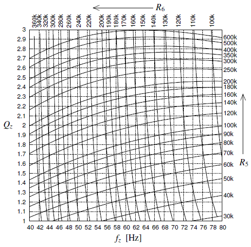
The resonant frequency (fz) and the mechanical Q value (labeled Qz) of the enclosed bass driver must be known by measurement or otherwise. Then the values for the two resistors are found by interpolating between the nearest curves. For example, if the needed operation parameters are fz = 70 Hz and Qz = 2.5, we obtain, by reading the contours, R5 = 220 kΩ and R6 = 125 kΩ. As can be seen, R5 affects mainly the Q value and R6 mainly the frequency.
When using speakers with built-in resonance compensation, active compensation is no more needed. In this case, the amplifier's frequency response can be leveled by making the zeros introduced by the equalizer cancel out the above-described 30-Hz cut-off. This canceling is achieved simply by setting fz = 30 Hz and Qz = 0.5 which makes the transconductance at audible frequencies next to flat. The point is not seen in the map, but the needed resistances are R5 = 32 kΩ and R6 = 750 kΩ.
Balance Stage
Potentiometer P2 acts as the balance control. Each channel has its own potentiometer on a common axis, connected so that when one is turned open, the other turns shut. Thereby, one avoids the interchannel crosstalk, possible in the usual balance control circuit, stemming from current partially drifting past the grounded slide. The effect of R7 is that attenuation at the potentiometer's middle position is about 3 dB when otherwise it would be 6 dB.
Baffle Step Options
A4 with its feedback forms the baffle step compensation stage and also acts as a buffer, feeding the volume potentiometer P4. With jumper (or switch) J1, one can select either an unmodified response (0) or one of the four compensation levels that are shown in the graphs below.
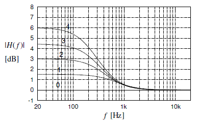
At position 4, low frequencies are boosted a full 6 dB, the different options being arranged at 1.5-dB spacing. Because, due to power response aberration, it is generally not needful to eliminate the baffle step wholly, option 3 or 2 is often the most appropriate for frequency balance.
The center frequency of the step has been set to approximately match an enclosure width of a good 20 cm. If the size differs much from this, the frequency can be scaled by changing the value of C6.
Offset Trim
By trimmer P3, one can reduce the direct current flowing to the load, stemming from the offset voltages of A4 and A5. However, due to the potentiometer between these stages, the direct current cannot be nulled entirely except at some specific position of P4.
Power Supply
The power supply has been implemented using the adjustable regulator LM338, whose current supplying capability is more than adequate for the purpose. Because negative regulator chips are not available for high currents, the negative side has also been realized with a positive regulator. The arrangement works anyway all well.
Using a regulated power supply also for the power amplifier is not so common today but is, however, well justified here because, besides avoiding hum problems, with a regulated supply the operating voltage range of the amplifier chip can be utilized much better than with an unregulated one.
It is vain to suspect anything such that a regulator circuit would not be able to deliver current fast enough in all possible transient situations. To prove this, it is enough that the voltage variations remain practically negligible with the highest load current and the highest operating frequency. The use of regulators does not endanger the amplifier's stability either, as long as the necessary bypass capacitors have been appropriately connected.
Moreover, regulation suits for a current-output amplifier better than for a voltage-output one because in the first-mentioned, the required peak currents are at the same power level much lower due to the fact that the reactivity of the load no more affects the instantaneous values of current.
The supply voltage has been set with resistors R18, R19, R21, and R22 to ±17.5 V, so that the same source can also be used for the operational amplifier chip, that can withstand ±18 V. Amplitude peaks are then able to reach ±15 V.
The values of C16 and C20 are much higher than usually in order to curb the power-on snap. The output terminals of the regulator develop a voltage of a good volt instantaneously after power-on, but due to the slow charging of these electrolytes via R20 and R23, the supply voltage reaches its full value only after a couple of seconds.
C22 must be a so-called class X capacitor, intended for mains voltage interference suppression. Ordinary capacitors should not be used in the place.
Boards
Below is shown the top layout view for a two-channel amplifier and its power supply, using the circuit boards that are found as PDF images here and here.
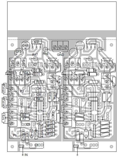
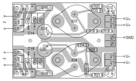
The components have been named only for one channel, but the other is furnished the same way. The rectangles marked with a screw head represent screw terminal cells. The inputs and jumpers J1 may be connected by means of pin headers. For some capacitors, there has been provided different pitch options. C10 and C11 are not seen in the picture but are situated on the copper side directly from the supply voltage pins of IC2 to the ground foil. The regulators are purposed to be fixed with their heat sinks on top of spacers above the board.
Connections
All external connections to the boards are purposed to be made using screw terminals except the inputs, for which are suggested gold-plated pin headers with corresponding female crimp terminals. To improve mechanical firmness, 3-way terminals have also been used for many 2-way connections.
For resistances R5 and R6, there are used 4-way screw terminals to enable series connection since it is unlikely that the needed resistances would coincide with commercial standard values. When mounting the resistors, one must remember to remove from their leads all adhesive residues stuck from the tape.
The wire strands should be tin coated since plain copper oxidizes quickly degrading contact reliability. It is well to check the tightness of the screws yet the next day after mounting, for they have a tendency to loosen a little.
The supply voltage wires can be drawn for both channels separately from the power supply board, the ground wire being common. All five should be bundled together to reduce inductances; and also in general, all wires should be kept as short as possible. From the GND terminal of the amplifier board is also drawn contact to the chassis.
The input signals are brought to the possible selector switch and the amplifier board by screened cables. To avoid ground loops, the bodies of the RCA connectors are isolated from the appliance chassis.
In the installation of the regulators, one has to see to it that the case, which forms the output terminal, has reliable contact with the pertinent copper foil, minding that the blackened heat sink surface or an oxidized copper surface may form an insulating layer. If needed, a separate short wire should be used.
Images & Thermal Design
Below are found images of the whole project, the amplifier side, and the power supply side. The heat sinks shown are adequate for normal listening though not necessarily for the hardest testing. Both the amplifier chips and the regulators are equipped with thermal shutdown features.
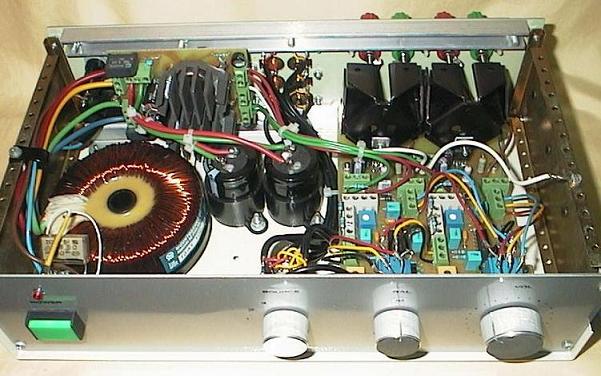
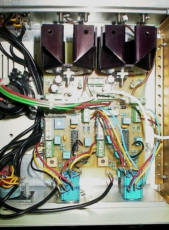
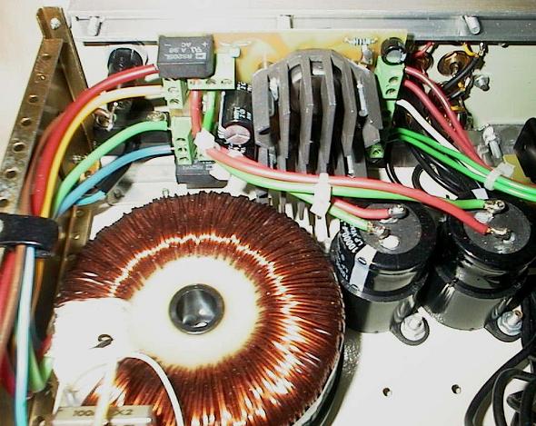
If a common heat sink is used for the amplifiers, it is advisable to isolate them electrically from the sink, so that it would not convey operation currents of the amplifiers. The heat sink is then connected to ground potential.
Quality Considerations
The best choice of dielectric material for the signal path capacitors C1, C3, C4, C5, and C6 is polypropylene, whose non-idealities are considerably lesser than those of polyester.
The selector switch and the potentiometers should be of higher than ordinary quality if they are desired to preserve their contacts still after years.
Getting More Power
By using TDA2050, the output power can be increased up to 25 W per channel, but this requires that IC1 must be provided with own supply voltage regulators, as it can withstand only ±18 V. R16 should then be decreased to 0.47 Ω, or even a little lower if more gain is desired.
For the TDA2050, a suitable target for the supply voltage is ±24 V. For the transformer secondary should then be chosen 2x24 V; and the sum R18+R19 should be set to 2.2 kΩ, as also R21+R22, regarding that this resistance consumes 0.22 W power. Heat sinking also needs then improvement from that seen above.
Reduced Build
If the included resonance and baffle step filters are not needed, they can be omitted and only the power transconductor portion (A5 with its associated components) can be built. Then, P4 can also be replaced by a fixed resistor of about the same value (from the noninverting input to ground). A coupling capacitor of 3.3 µF (plastic) should yet be added at the input to block possible DC from the feeding source.
Here, the supply voltages can be increased close to the maximum rating of the IC used. Regulation is not a necessity, but then the turn-on/off transients may have to be dealt with differently.

