Low-Distortion Class-A Transconductor Amplifier
with Voltage Regulators as Output Devices
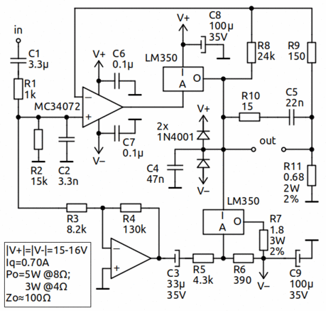
This is a low-power, low-distortion class-A transconductor project using LM350 adjustable voltage regulators as the output devices. It is capable of delivering 5 W into 8 Ω load and 3 W into 4 Ω with 15-16 V supples and a quiescent current of 0.70 A. A dual op-amp MC34072 is used to control the regulators. The output impeance has been set to about 100 Ω. Due to the overall feedback loop and the very accurate output devices, the total harmonic distortion is less than 0.001% at the mentioned full power levels (1kHz).
An outstanding characteristic of this circuit is that it is completely silent during power up/down, thus allowing to dispense with any transient muting circuitry.
If the op-amp type becomes unavailable, TL072 can be used as a substitute with minor effect on performance. (Do not, however, swap for the popular NE5532; it has too high bandwidth for this.)
Operation
The input circuitry limits the -3 dB bandwidth to somewhat less than 60 kHz. The lower regulator is operated as a voltage-controlled current sink and provides half of the needed output current without feedback. The quiescent current is determided by R7 and is very stable. While this current contains a small amount of ripple deriving from the negative supply voltage, it gets well suppressed by the feedback loop around the upper regulator, which provides the other half of the output current as an unity-gain buffer. The feedback amplifier also operates in class A, as it draws only 50 µA direct current from the regulator's adjustment pin.
The feedback signal is a mixture of voltage feedback via R8 and current feedback from the current sensing resistor R11 via R9. With the values given, the output impedance is just over 100 Ω at low and mid frequencies and slightly less at the top end. This is enough to reduce current-derived distortions by about 23 dB at 8 Ω load and even 28 dB at 4 Ω. A small amount of voltage feedback helps to sustain adequate phase (stability) margin with highly inductive loads and also prevents the output voltage from saturating in case the load is disconnected.
The purpose of R10 with C5 is to provide resistive loading at high frequencies to ensure loop stability regardless of varying speaker loads. Together with C4, they also bypass some of the HF noise of the regulators. C4 was also found to enhance HF stability. The diodes are for protecting the regulators in severe overdrive conditions.
Layout & Cooling
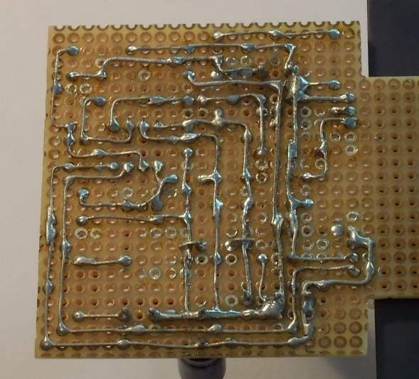
A matrix board layout for a single amplifier is shown below. Most part of the wiring can be established using the component leads. It is advisable not to differ much from this layout structure, for at least the proper routing of the supply bypass capacitors and C4 was found somewhat crirical.
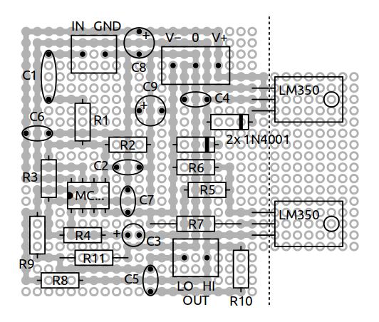
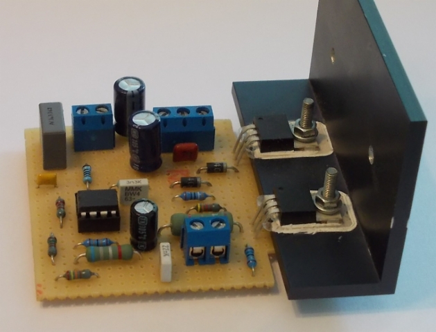
The regulators dissipate 10-11 W each when idling, so a bulky heat sink is required. Their tab is connected to the output pin and hence needs electrical insulation. Do not, however, use any silicon pads or suchlike for this, for they are totally unsuitable for a TO-220 package and can even warp the tab when tightened.
The L-piece seen below is only to facilitate connection to the actual heat sink. The piece is lifted from the board by sizable washers. Wirings that carry high currents have been fortified by excess tin or thicker leads.
Powering
Regulated power supply is not necessary, but it is advisable to use two 4700µF/35V electrolytes in parallel on both sides (+/-) per one channel. If the voltage exceeds 16 V (2x12V trafo), one can add some series resistance between the capacitors (CRC filtering). This also attenuates ripple.